Skip to content
  • Applications & Solutions
      • 5g-icon5G
      • packaging-assembly-iconPackaging & Assembly
      • automotive-iconAutomotive
      • lithography-iconLithography
      • sensor-manufacturing-iconSensor Manufacturing
      • paint-coatings-iconPaint & Coatings
      • lasers-iconLasers
      • substrates-iconSubstrates
      • ceramics-iconCeramics
  • News
  • Careers
  • About Us
  • Sustainability
  • Contact Us
  • Applications & Solutions
    • 5G
    • Packaging & Assembly
    • Automotive
    • Lithography
    • Paint & Coatings
    • Lasers
    • Substrates
    • Ceramics
  • News
  • Careers
  • About Us
  • Sustainability
  • Contact
  • Applications & Solutions
    • 5G
    • Packaging & Assembly
    • Automotive
    • Lithography
    • Paint & Coatings
    • Lasers
    • Substrates
    • Ceramics
  • News
  • Careers
  • About Us
  • Sustainability
  • Contact

Efficient Barrier Coatings for Electronics

Electronic materials rely on all components working together seamlessly. There is no room for a mistake when it comes to the manufacture of electronics, with

Read More »

Characteristics of Dry Film Permanent Bonding

Dry film permanent bonding is used to bond the 3D TSV, or Through-Silicon-Vias as well as two dimensional wafer bonding applications. The film comes in

Read More »

Performance Properties of Thermally Conductive Adhesives

Thermal grease, or thermally conductive adhesive, is used in the semiconductor industry to assist a heat sink to draw heat away from semiconductor components like

Read More »

Importance of Low Gas-Permeable Silicone

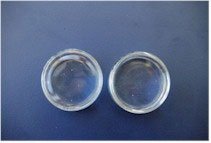
There are many problems that can occur when silicone encapsulants that have a high gas permeability are used as a barrier coating for applications having

Read More »

Uses of Nano-Imprint Templates

Nano-imprint templates can be used in the development of many devices, such as semiconductors, storage devices, optical parts, biochips, and various MEMS devices. One benefit

Read More »

Functions of Die Attach

The die attach process is a critical step in the manufacturing of electronic materials, and one that presents continual challenges to the industry. In the

Read More »

Benefits of Contrast Enhancement

Contrast enhancement material, or CEM, is a photo-bleachable material applied to the photoresist surface then removed with DI water pre-wet. There are many benefits to

Read More »

2.5D and 3D Packaging Material Technologies

IC packaging, or integrated circuit packaging, is the final stage of semiconductor device fabrication. The block of semiconducting material is enclosed and encased in a

Read More »
LED Encapsulant Materials - Shin-Etsu MicroSi

Choices for LED Encapsulants

As the LED, or light emitting diodes, lighting market continues to grow at an increasingly robust pace, the demand for LED encapsulants and underfill materials

Read More »

Using Photoresist and E Beam Resist Technology

A photoresist is a light-sensitive material used in photolithography to create a patterned coating on a surface. Some applications of photoresist are: microelectronics, patterning and

Read More »
« Previous Next »
  • About Us
    • Shin-Etsu Chemical Co. LTD
    • Other Shin-Etsu Companies
    • Research & Development
  • Sustainability
  • Legal / Regulatory
    • ISO Certified
    • General Terms and Conditions of Sale
  • Applications & Solutions
    • 5G
    • Automotive
    • Advanced Packaging Materials
    • Paint & Coatings
    • Sensor Manufacturing
    • Substrates
    • Ceramics
    • Lasers

Follow Us

  • Careers
    • Core Values
    • Equality, Diversity & Inclusion
    • Benefits
    • Opportunities
  • Document Center
    • Press Releases
    • Data Sheets
    • Blog
  • Contact
Copyright 2026, ShinEtsu Microsi

|  Privacy Policy | Terms of Use

Get In Touch with MicroSi

  • This field is for validation purposes and should be left unchanged.
×

Cart